Microelectronics Research at Paderborn University
Within the program “Research Laboratories Microelectronics Germany (ForLab)” of the German Federal Government’s Framework Programme for Research and Innovation 2016–2020, the research group “Power Electronics and Electrical Drive Technology (LEA)” at Paderborn University was able to significantly upgrade and expand its laboratory infrastructure. The investment, entitled “Integrated Power Electronics Laboratory for Future WBG Applications with Maximum Miniaturization and Efficiency,” contributes to establishing a high-performance and future-proof infrastructure that enables research on WBG-based systems—from development and practical implementation to functional and reliability analysis. WBG stands for “Wide Band Gap” and refers to novel semiconductors with a large band gap between the valence and conduction bands.
Compared to conventional silicon-based power electronic semiconductors, WBG semiconductors offer significant advantages such as higher thermal conductivity, higher breakdown voltages, and much faster switching speeds. This enables the realization of power electronic systems with high switching frequencies. As a result, passive components such as inductors, transformers, and capacitors can be designed more compactly, which on the one hand keeps overall component costs (despite typically higher semiconductor costs) at a level comparable to silicon-based systems, and on the other hand significantly increases power density or correspondingly reduces the overall system volume. Especially in the context of mobile applications such as electromobility, WBG-based power electronic converters offer considerable potential for energy savings, as, among other factors, the total mass of power electronic systems can be significantly reduced. For these reasons, WBG semiconductors represent an important driver of innovation in power electronics.
Infrastructure | Environment |
ForLab FutureLab PE
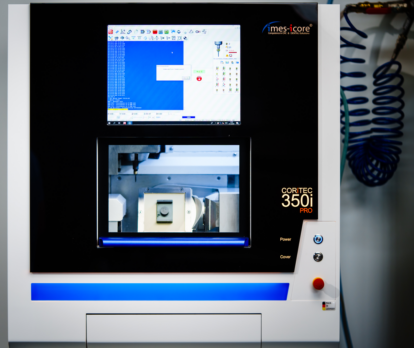
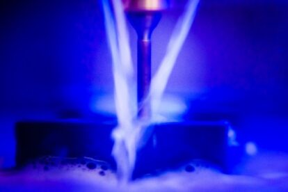
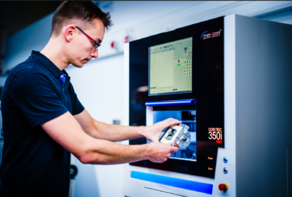
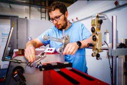
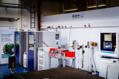 CNC ferrite milling machine for the production of complex core geometries for application-specific windings
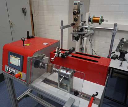
CNC winding machine for the precise fabrication of application-specific windings
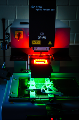
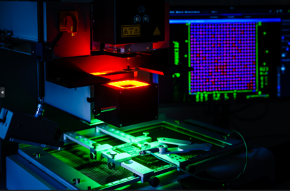
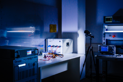
Switching-loss test bench for the characterization of fast-switching wide bandgap semiconductors 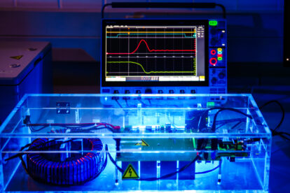 Photo: André Wirsig Rework station for assembly and disassembly of highly demanding SMD packages
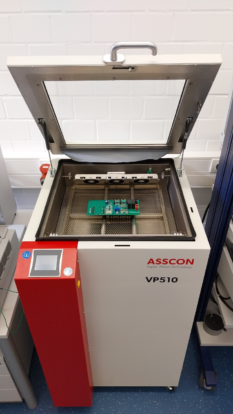
Vapor-phase soldering system for achieving highly homogeneous temperature distributions
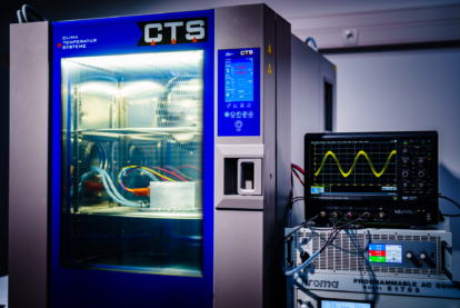
Climate chambers for testing prototypes, assemblies, and components under special environmental conditions or accelerated aging tests (thermal cycling)
EMC laboratory for conducted emissions 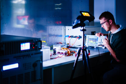
Calorimetric measurement chamber for precise loss determination of assemblies and systems 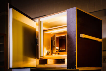 | Chair of Power Electronics and Electrical Drive Technology
Chair of Sensors, Flexible Electronics, and Integrated OpticsHeinz Nixdorf Institute – Group for Circuit Technology, Nanoelectronics, and NanophotonicsAssociated projects:
|
Education | |
Institute of Electrical Engineering and Information TechnologyBachelor’s program Electrical Engineering | |