Microelectronics Research at the University of Duisburg-Essen
Microelectronics research at UDE focuses on terahertz and millimeter-wave devices and modules for applications in communications, high-resolution radar sensing, material identification, as well as medical and biological imaging. Innovative semiconductor devices based on indium phosphide (InP) and gallium nitride (GaN) are fabricated in-house and investigated in a wide range of application scenarios. This includes expertise in heterostructure synthesis using metal-organic chemical vapor deposition (MOCVD) and molecular beam epitaxy (MBE), device physics, MMIC design and chip fabrication, as well as packaging and module technology for frequencies in the terahertz range (300–3000 GHz). As a result, THz transmitters and receivers with record data rates, highly efficient and compact THz sensor heads, and broadband transistor circuits are being developed—also in cooperation with foundry partners within the Research Fab Microelectronics Germany (FMD), through a joint lab with FBH, Berlin, and in collaboration with Fraunhofer IMS, Duisburg. Applications of terahertz and millimeter-wave technologies in sensing and communications are pursued at UDE within several funded networks and consortia, including DFG SFB/TRR 196 MARIE, BMBF 6G-HUB 6GEM, and EU MSCA ITN Teraoptics.
Infrastructure | Environment |
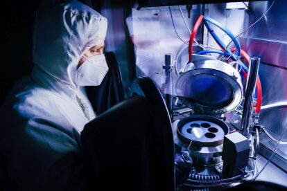
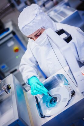
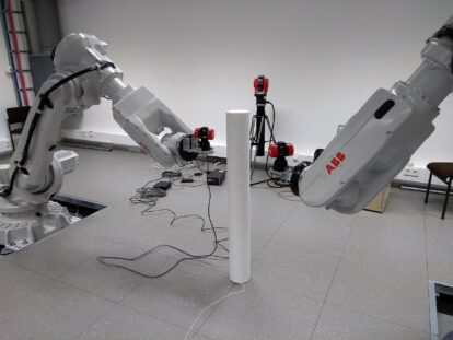
Center for Semiconductor Technology and Optoelectronics (ZHO), cleanroom (450 m²) with a complete technology chain (materials, chip processing, packaging and module technology), ForLab SmartBeam. Epitaxy of InP and GaN, electron-beam lithography with 10 nm resolution, plasma etching, plasma CVD, ALD, metallization, optical lithography, flip-chip, wire bonding, fiber alignment. Field-emission SEM, HR-XRD, AFM, confocal microscope, Hall measurements, photoluminescence. Software for physical device modeling, electronic and photonic circuit design. Free-space (robotic) S-parameter measurements and wafer probing up to 1.5 THz, spectrum analysis up to 750 GHz, low-level DC, TDS THz. Prof. Dr. Nils Weimann  Prof. Dr.-Ing. Andreas Stöhr Prof. Dr.-Ing. Andreas Stöhr  Prof. Dr.-Ing. Thomas Kaiser Prof. Dr.-Ing. Thomas Kaiser  | Chair of High-Frequency Electronic Devices (BHE)
Chair of Optoelectronics (OE)
Chair of Digital Signal Processing (DSV)
Projects & NetworksSFB/TRR 196 MARIE EU MSCA ITN Teraoptics EU KDT JU RIA Move2THz (website under construction) BMBF 6G-HUB 6GEM NRW research network terahertz.nrw |
Education | Other |
Core courses
Master’s courses
| DFG Core Facility ICAN for Materials AnalyticsUDE NanoSchoolLab and UDE QuantumSchoolLab(funded by REACT-EU-zdi) |