Mikroelektronikforschung an der Technische Universität Chemnitz
An der Fakultät für ET/IT sind insbesondere die im Zentrum für Mikro- und Nanotechnologien (ZfM) organisierten Lehrstühle
- Professur Smart Systems Integration,
- Professur Schaltkreis- und Systementwurf,
- Professur Mikrosysteme und Medizintechnik,
- Professur Mess- und Sensortechnik,
- Professur Elektronische Bauelemente der Mikro- und Nanotechnik,
- Professur Werkstoffe und Zuverlässigkeit mikrotechnischer Systeme,
- Professur Leistungselektronik sowie die
- Professur Materialsysteme der Nanoelektronik in der Mikroelektronikforschung aktiv.
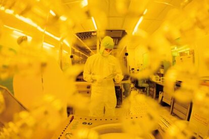
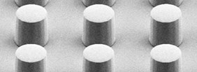
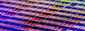
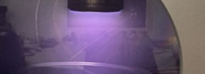
Die technologischen Prozesse für eine Waferbearbeitung auf vorrangig 150 mm und 200 mm Wafern werden in den Reinraumbereichen mit insgesamt 1300 m² Fläche (ISO4…ISO6) bereitgestellt. Sie umfassen die gesamte Prozesskette von der Schichtabscheidung für vielfältige Materialien, Hochtemperaturprozesse, Oberflächenbearbeitung, Mikro- und Nanostrukturierung bis zum Waferbonden sowie eine umfangreiche Technik zur Analytik.
Schwerpunkte der Forschung sind
- Design und Simulation von Materialien, Komponenten und Systemen
- Wissensbasierte Prozessmodelle
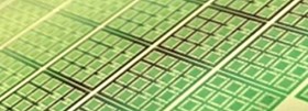
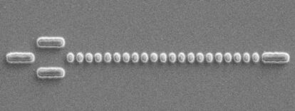
- Mikro- und Nanotechnologien, Integration neuer Funktionsmaterialien
- Technologien und Komponenten für Mikro- und Nanosysteme
- Test und Zuverlässigkeit
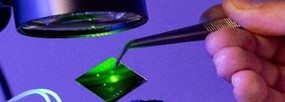
Das Forschungszentrum für Materialien, Architekturen und Integration von Nanomembranen (MAIN) ist eine zentrale Einrichtung der TU Chemnitz und verfügt ebenfalls über ausgewählte Anlagentechnik mit Fokus auf die explorative Erforschung der grundlegenden physikalischen und chemischen Eigenschaften sowie die Erschließung des ingenieurwissenschaftlichen Anwendungspotentials flexibler nanostrukturierter Membranen (‚Nanomembranen‘) als neuartiger Materialklasse.
Infrastruktur | Umfeld |
Forschungsreinraum Zentrum für Mikro- und Nanotechnologien
Forschungszentrum für Materialien, Architekturen und Integration von Nanomembranen (MAIN)
| Fakultät für Elektrotechnik und Informationstechnik
Forschungsfelder am Zentrum für Mikro- und Nanotechnologien: Advanced Micro and Nanopatterning
Molecular Micro- and Nanosystems
Spintronics – XMR sensors and spintronic films stacks
|
Lehre | Projekte |
Bachelorstudiengänge Vom Abitur zum Bachelor
Masterstudiengänge Vom Bachelor zum Master
|
|
Veranstaltungen | Sonstiges |
| Leistungszentrum Funktionsintegration für die Mikro-/Nanoelektronik Dresden/Chemnitz
|